
Nanowires (NWs) can be defined as cylindrical-shaped nanostructures with diameter in the order of nanometres and that very recently, have been attracting the attention of scientific community due to its unique set of properties which were found to be promising to compose the next generation of nano-electronic devices.
One particular challenge is the synthesis and design of new materials that can be used to manufacture new transistors at the nano-scale, thus revisiting and giving extra-life to the hyper-saturated Moore’s law for electronics and computers processor. In this context, one-dimensional nanowires have been recently considered the most promising candidates.
However, semiconductor materials are generally produced upon the incorporation of dopants by using ion implantation: a technique that can introduce several different types of defects within the material.
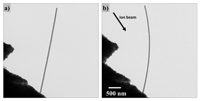
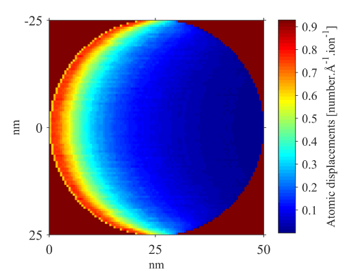
Our research group led by my french friend O. Camara, has been focusing its attention to the phenomenon of Ion-Induced Bending (IIB) of nanowires and in a recent publication at the Advanced Materials and Interfaces journal, we have demonstrated that the IIB phenomenon can be mitigated (AND EVEN REVERSED!) by means of Solid-Phase Epitaxial Growth. In order to support the discussion, we have developed a MATLAB-based implementation of the Stopping and Range of Ions on Matter (SRIM) that now is known as IDRAGON: Ion Damage and RAnge in Geometry Of Nanowires. For the whole nanowires community interested in to get a copy of our code, fell free to contact me (m.a.tunes[at]physics.org).
Featured image credits on the top of the post: CVD equipment coorporation.

Interesting article focusing a recent published work by Matheus Tunes.
LikeLike